The preferred method of introducing electrical dopants in the chip fabrication process is to mask off the regions of interest, bombard the silicon with a high energy beam of the required dopant source, and then anneal the wafer; heating it to a high temperature and cooling it in a controlled manner.
Huge advances in lithography (the masking step) have enabled the lateral feature sizes of the doped regions to be scaled to a few nanometers (billionths of a meter), so that billions of transistor devices can be put on a single silicon wafer.
In fact, the advances in the lateral resolution of lithography are now outpacing the ability to control doping in the vertical direction. The various anneals and oxidation steps in most fabrication processes cause the profile of implanted dopants to “smear out” (diffuse), which can in turn impair the performance of the silicon, for example by reducing the current or by increasing the device-to-device variability.
One of the most common steps in most semiconductor processes is an oxidation of the silicon surface. It is well-known that this process injects many imperfections (interstitials) into the silicon. This flood of interstitials speeds up the diffusion of dopants such as boron and phosphorus, so that, like the action of waves on a sandcastle, the original doping profile is significantly broadened.
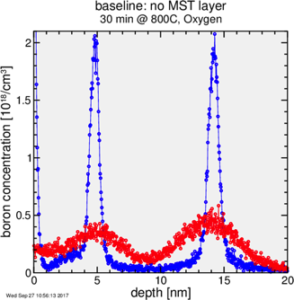
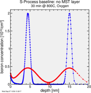
The dopant broadening under oxidation is illustrated in the experimental results of figure 1.
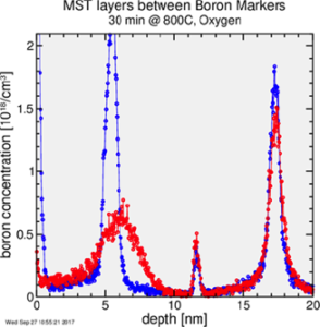
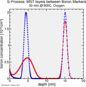
Atomera has demonstrated that its MST® technology can be used to inhibit the vertical smearing of dopants, with up to an order of magnitude better vertical control than current processes. We believe that this result is highly significant for the design of many silicon devices, and can be used to considerably reduce the variability of various parameters, allowing tighter specifications, reduced power consumption and improved yield. Figure 2 shows how Atomera technology can be used to sculpt the doping profiles, in this case to retain the doping level in the right hand peak. It shows the original dopant (in blue), and the dopant after processing (in red). This ability to manage dopant profiles is very valuable to semiconductor manufacturers because it can positively impact chip performance.


Synopsys is highlighting the Atomera technology to many of the world’s TCAD engineers during their October Far East seminar series timed to accompany the new Sentaurus release.
