Better matching with MST
Last year I wrote about one of the unique attributes of the MST® technology in the design and implementation of semiconductor doping profiles. MST can facilitate “precision doping profiles” which are “frozen” or “anchored” in place and do not smear out after subsequent oxidations and anneals. It does this by blocking some of the common diffusion mechanisms.
We have recently obtained some excellent results with one of our analog partners, who have allowed us to reproduce the data shown below.
Engineered doping profiles are of strong interest in analog and mixed signal circuit design. It is important that when needed, transistors (usually adjacent) which are designed to be identical do indeed have matched parametric performance. Examples of circuits where minimizing mismatch is critical range from analog circuits incorporating current mirrors, A-D and D-A converters, SRAM cells and DRAM periphery sense amplifiers. In general, mismatch affects the trade-off between speed, power and accuracy. In SRAM, mismatch directly affects the minimum voltage for reliable operation and hence the low power limit. In DRAM sense amplifiers, mismatch sets a limit on the discrimination of sensed current/voltage and hence on the scalability (and size) of the periphery circuit. In some low noise circuits, for a given bandwidth (speed), mismatch can set the performance threshold rather than the noise limit.
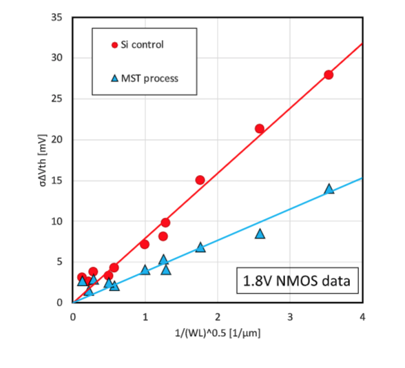
The degree to which such “identical” transistors are mismatched is characterized using a plot known as a Pelgrom plot, after a classic paper by Marcel Pelgrom and co-workers from Phillips Research Labs. A test chip is designed with large numbers of nominally matched pairs of transistors with different widths (W) and gate length (L). The difference in the threshold voltage, Vt, of the matched pairs is measured (ΔVt), and the standard deviation (σ) of the distribution of the ΔVts for the set of matched pairs is plotted against the inverse square root of the product of L and W. The slope of this plot, Avt, is a figure of merit for a given technology.
An example of such a Pelgrom plot is shown in Figure 1.
In order to stay below a maximum allowable ΔVt variation, designers are forced to increase the overall size of the transistor. Depending on the number of critical matched devices, such a strategy will increase die size, and hence cost. In general, moving to larger transistors also impacts speed and performance.
The recent data with our partner illustrates this.
To put this result in context; this means that the same absolute ΔVt variation in the optimized MST transistor can be achieved in a transistor of only a quarter of the area of the baseline device!


