Atomera Patent Portfolio
By Frank Laurencio, CFO
Atomera has built an extensive patent portfolio since its founding in 2001, with our first US patents filed in 2003, and counterparts filed outside the US shortly thereafter. As a technology licensing company, our IP is a critical asset, so in this post I offer some insight into how we built our patent portfolio and how we are leveraging our intellectual property to enhance shareholder value.
Early Patent Activity
When Robert Mears founded Atomera in 2001, he had already invented materials technology that revolutionized long-haul fiber optics, most notably with his invention of the erbium-doped fiber amplifier, or EDFA (you can read the IEEE Spectrum magazine’s write-up on it here). Atomera was based on the idea that similar approaches to doping crystalline substrates could benefit semiconductors. Accordingly, our early patents centered around altering the crystal lattice structure of semiconductor materials. Today we are engaged with semiconductor industry participants to understand how MST might be used in the devices they manufacture. So, while our early Atomera patents addressed concepts such as electron mobility in a MOSFET, our more recent patents cover a wide variety of device architectures that we believe will benefit most from MST.
Lean Years
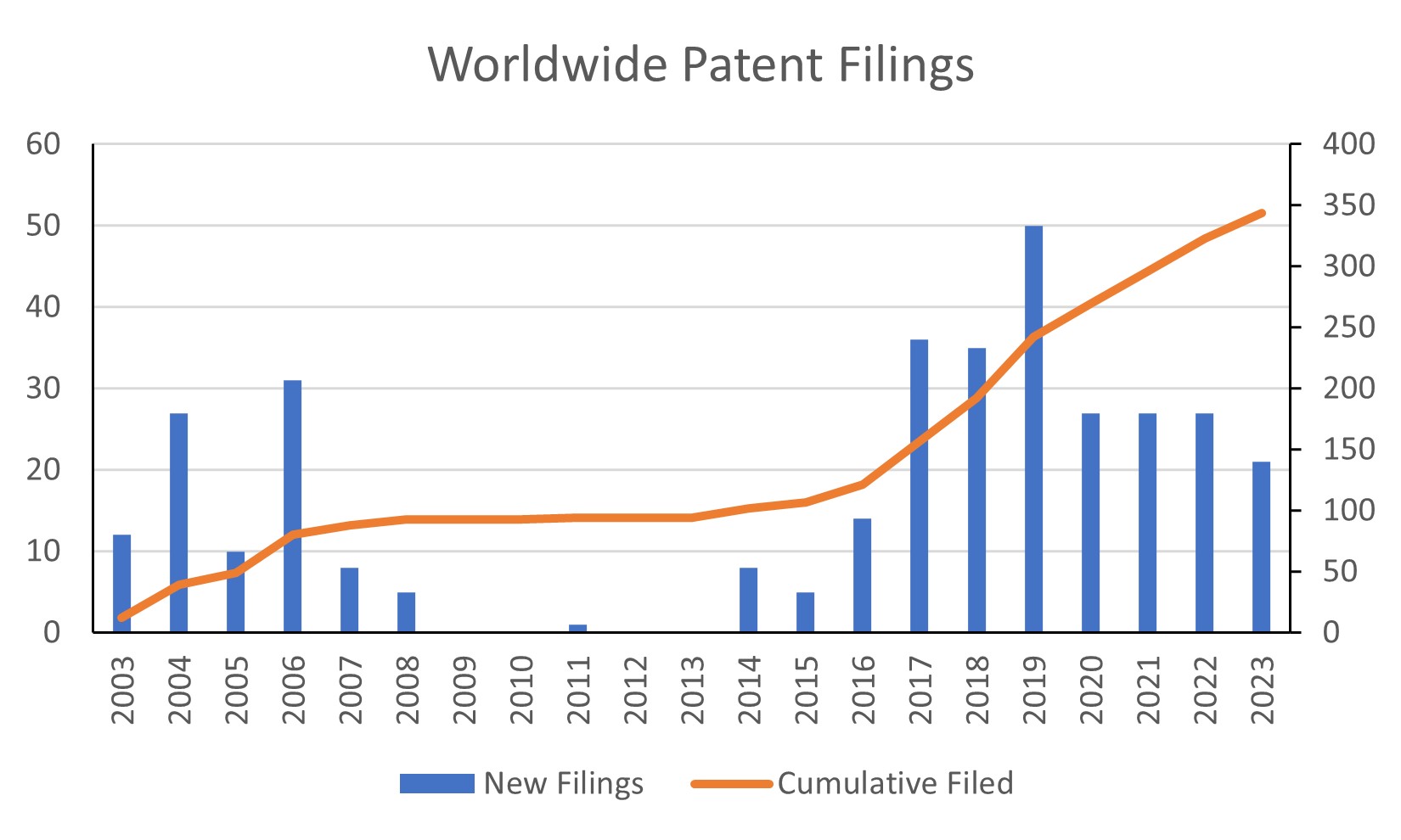
To understand the timing of patent issuances and expirations, it is useful to look back at how our patent filing activity developed over the years. As the bar chart below shows, Atomera was very active in filing patents in the period from 2003-2007 when we filed 88 patents worldwide. Some of those early patents have started to expire. In the seven years after that (2008-2014), we filed only 14 patents. This was not due to a lack of innovation but was a response to the challenging funding environment faced by semiconductor startups, coupled with the global financial crisis. When the company recapitalized in preparation for our IPO in 2016, patenting activity started to pick up again. Between January 1, 2016 and now and we have filed 237 patents worldwide as compared to 107 patents in the 13 years from 2003-2015 – more than doubling our patent filings in about half as much time.
The number of patents we hold at any point in time can ebb and flow based on when we submit filings, patent office application processing timeframes, and expirations after the 20-year term. The elevated level of patent activity since our IPO provides patent protection into the 2040’s and we intend to continue this strong trajectory.

Our Strategy for Commercializing MST
As a technology licensing company, our business model relies on both our patent portfolio and our proprietary trade secrets. Patents are public documents that anyone can study, but they protect inventions by granting exclusive rights for a limited time period. Trade secrets, on the other hand, safeguard confidential and valuable information that provides a competitive edge. So while our patents protect the devices made using MST and the methods for doing so, the recipes for depositing MST film on wafers are not patented but are protected as trade secrets which we only divulge to customers under strict contractual protections. Unlike patents, which by law are limited to 20 years, trade secrets have no expiration. When we enter into a license agreement with a customer, we license both our patents and trade secrets to them – both types of IP are necessary for a customer to capitalize on the benefits of MST.
As Atomera has evolved from our roots in basic materials science to a value-add partner for semiconductor makers, our patents and know-how have also broadened to protect our innovations in the many areas that benefit from MST Technology.
Our engineers continue to innovate and protect their inventions with our powerful combination of patents and trade secrets, both in the areas we currently focus on and in new, related fields. Atomera is a very different company today than when we started out focused on basic materials science. We are engaged with companies across the full range of semiconductor process technologies and we have the patents and know-how covering our innovations in those areas, providing a much stronger and more valuable set of IP assets on which to build our licensing business.
