Applications
Analog & PowerSmaller Die Sizes mean Lower Cost for Analog and Power
Atomera’s MST-SP technology demonstrates breakthrough performance and density improvements to power and analog devices. Thanks to the combination of dopant profile engineering and mobility improvement made possible by MST, the MST-SP technology can reduce die size of PMICs and other 5V devices by up to 20% without degrading reliability or efficiency.
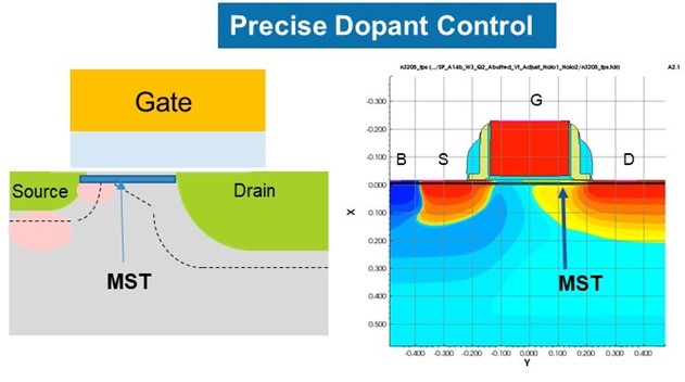
Atomera’s MST film enables precise doping control, as shown in the figure above, while also enhancing carrier mobility. Combined with the asymmetric “SP” device profile, the result is a substantial enhancement to Idlin and BVDSS, as well as enabling further Lg scaling.
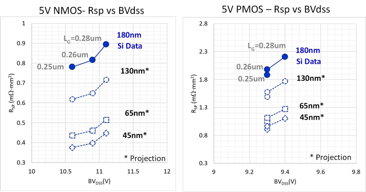
Compared to baseline symmetric 5V NMOS analog transistors, MST-SP has been demonstrated to offer 3x lower specific on resistance (Rsp). Compared to asymmetric 5V analog transistors of similar design, MST-SP offers up to 25% lower Rsp at the same breakdown voltage, BVDSS. The MST-SP breakthrough also applies to 5V PMOS and has applications beyond 5V analog to many other silicon devices, including planar CMOS devices.
By enabling further gate length scaling, MST-SP brings even greater benefits to scaled analog nodes. Projections with design rule scaling for 130nm BCD processes show 40% lower Rsp compared to a 180nm BCD process without MST
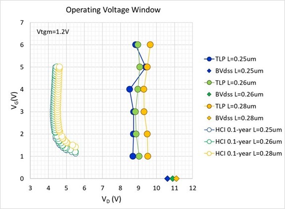
The device improvements do not require any sacrifice in quality – the MST-SP device is robust and meets standard commercial reliability requirements.


